Learn to design electric circuits. Enroll today to learn from a PCB designing expert.
Course Duration
30 Hrs.Live Project
2 ProjectCertification Pass
GuranteedTraining Format
Live Online /Self-Paced/ClassroomWatch Live Classes
Speciality
200 +
Professionals Trained3 +
Batches every month20+
Countries & Counting100+
Corporate Served- A PCB (Printed Circuit Board) is thin fiberglass or laminated board that contains self-contained interconnected electrical components. It connects and supports all of the electrical components electrically and mechanically. It is basically used for conductive tracks or laminated copper sheets. If you want to acquire detailed training in this course, then approaching an educational structure will be suitable for your career.
- Croma Campus is one of the best providers of PCB Designing Training in Delhi that targets to provide complete assistance and help to secure a job in their dream organizations. Having complete knowledge of the subject is necessary, but you also need to have practical knowledge of the same. With our course, you can have excellent practical knowledge that can lead you towards your dream job hence you secure a better future.
PCB Designing Training in Delhi

- The Printed Circuit Board (PCB) is an important element amongst electronic gadgets, that are highly used either for domestic use or industrial purposes. During the tenure of your PCB Designing course, here’s the list of our course objectives. To analyse this course in detail, you should get in touch with a good PCB Designing training institute in Delhi.
Candidates can analyse different aspects of Printed Circuit Board Design and fabrication.
In fact, candidates can learn various types of PCBs. Schematic Design. entry Rules for Schematic Entry, Component Layout methods.
You will also receive sessions regarding placement rules and routing Techniques for Single-Sided boards.
Our trainers will help you to know the post-processing of design and Fabrication documents.
Moreover, after completing this PCB circuit design online training course, students can design and fabricate their own PCB for their Project and can also work in PCB Designing and Fabrication area.
- It is one of the most evolving fields and offers you a great salary structure as well. So, you genuinely don't have to worry about the salary and job post imbibing this accreditation. Moreover, if your interest genuinely lies in this direction, then getting started with PCB Designing course will be suitable for your career.
The average Printed Circuit Board Designer III salary in the United States is $85,306 as of May 2022, but the range typically falls between $77,111 and $102,584.
Salary ranges can vary widely depending on many important factors, including education, certifications, additional skills, and the number of years you have spent in your profession.
The range surrounding that average can vary from a person’s experience, knowledge, salary, and pay package.
- Well, at the moment, PCB Designing training institute in Delhi has been in demand because of its exceptional features, and scope. A PCB designer’s job is very important when it comes to the creation of a product and its inner workings. Of course, getting into this career is not easy because you need to learn about all of the different elements that go into printed circuit board design and much more.
To get you started and help to launch your career as a PCB designer, we have put together some tips.
The future of PCB designers is truly very bright. There are plenty of indications from the market that show there are a lot of opportunities after your PCB circuit design training course.
With competitive growth in consumer electronics and automotive industries, the thrive for making new cool, “smart” and sexy products is increasing.
- The Printed Circuit Board (PCB) is very important in all electronic gadgets, which are used either for domestic use or for industrial purposes. PCB design services are used to design electronic circuits. Apart from electrically connecting, it also gives mechanical support to the electrical components.
The PCB designs can be created both manually and automatically. Manual layouts are created with the help of CAD drafting, and the automatic router helps in the creation of the designs automatically.
The designers usually prefer the manual way of designing, since they can implement their own ideas and techniques in them.
PCBs are the core component in almost all electronic gadgets including cell phones and computers and laptops. With the increase in demand, the number of PCB services is on the rise.
A few among those listed on top are the OrCAD PCB design and the Altium PCB design.
- Post completing the PCB Designing Training in Delhi, you are likely to perform a range of job roles and responsibilities.
Work with the project team in understanding circuit requirements and limitations.
Develop design documentation and requirements specifications for assigned projects.
Provide support to PCB engineering, manufacturing, and packaging teams when required.
Review and recommend improvements to existing designs.
Assist in preparing test procedures and developing test fixtures to verify PCB functions.
Stay updated with the latest design techniques.
Perform component placement and maintain integrity between components.
- At the moment, numerous companies are looking for skilled PCB Designers, as there is a huge demand and work for them, yet the grant is quite low. So, if your interest lies in this field, then you should get started with a well-established PCB Designing training institute in Delhi.
For electronics experts seeking core employment, PCB circuit design is one of the greatest possibilities.
In India and overseas, the tool offers a variety of employment roles with outstanding career progression and salary incentives.
Intel, Qualcomm, Nvidia, Samsung, Broadcom, AMD, ARM, IBM, Cisco, Brocade Network Solutions, and Juniper Networks are just a handful of the big international businesses.
For freshers, you can find jobs in digital verification, physical design, bespoke layout, and mixed-signal verification.
- Croma Campus is one of the best providers of PCB Designing Training in Delhi. Over the years, it has made a remarkable place for itself amongst its contemporaries.
Our trainers will consecutively guide you to select the certification as per your educational background and desired growth.
You will be explained about various levels of certifications also.
Post the completion of the course, our trainers will help you to appear in front of huge established companies.
Croma Campus also holds a series of positive reviews of its past students, and that’s why it is so popular amongst the educational industry.
Why you should enrol in PCB Designing course?
By registering here, I agree to Croma Campus Terms & Conditions and Privacy Policy
 Course Duration
30 Hrs.Flexible Batches For You

19-Apr-2025*
- Weekend
- SAT - SUN
- Mor | Aft | Eve - Slot

21-Apr-2025*
- Weekday
- MON - FRI
- Mor | Aft | Eve - Slot
16-Apr-2025*
- Weekday
- MON - FRI
- Mor | Aft | Eve - Slot
19-Apr-2025*
- Weekend
- SAT - SUN
- Mor | Aft | Eve - Slot
21-Apr-2025*
- Weekday
- MON - FRI
- Mor | Aft | Eve - Slot
16-Apr-2025*
- Weekday
- MON - FRI
- Mor | Aft | Eve - Slot
Want To Know More About
This Course
Program fees are indicative only* Know more
Timings Doesn't Suit You ?
We can set up a batch at your convenient time.
Program Core Credentials
Trainer Profiles
Industry Experts
Trained Students
10000+
Success Ratio
100%
Corporate Training
For India & Abroad
Job Assistance
100%
BATCH TIMING
As per your requirementFOR QUERIES, FEEDBACK OR ASSISTANCE
Contact Croma Campus Learner Support
Best of support with us
PCB Designing Certification Training Programs
PCB Designing Certification TrainingPrograms
Mock Interviews
Prepare & Practice for real-life job interviews by joining the Mock Interviews drive at Croma Campus and learn to perform with confidence with our expert team.Not sure of Interview environments? Don’t worry, our team will familiarize you and help you in giving your best shot even under heavy pressures.Our Mock Interviews are conducted by trailblazing industry-experts having years of experience and they will surely help you to improve your chances of getting hired in real.How Croma Campus Placement Process Works?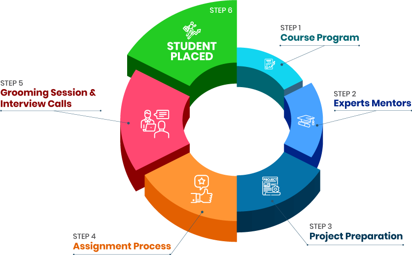
Phone (For Voice Call):
+91-971 152 6942WhatsApp (For Call & Chat):
+91-9711526942Projects
Batch Request
SELF ASSESSMENT
Learn, Grow & Test your skill with Online Assessment Exam to
achieve your Certification Goals

FAQ's
To turn into a successful PCB Designer, you need to know this subject deeply and acquire its legitimate certification.
Yes, it's one of the most suitable careers to choose from as it offers you ample opportunities to learn new things about this direction.
The PCB design is hugely in demand in the market with competitive growth in consumer electronics and the automotive industry, which thrive for making new digital products for the consumers.
Well, a PCB Designer is accountable for utilizing computer software programs to design the layout for these respective printed circuit boards, corroborates with engineers on the creation of 3D models of circuit boards, develops PCB design guidelines, and drafts plans for manufacturers respectively.
There are several steps involved in PCB designing, and some of them are as follows- Understand the electrical parameters, create the schematic, utilize a schematic capture tool to create your PCB layout, design your PCB stack up, define design rules and requirements, etc.

- - Build an Impressive Resume
- - Get Tips from Trainer to Clear Interviews
- - Attend Mock-Up Interviews with Experts
- - Get Interviews & Get Hired
If yes, Register today and get impeccable Learning Solutions!.

Training Features
Instructor-led Sessions
The most traditional way to learn with increased visibility,monitoring and control over learners with ease to learn at any time from internet-connected devices.
Real-life Case Studies
Case studies based on top industry frameworks help you to relate your learning with real-time based industry solutions.
Assignment
Adding the scope of improvement and fostering the analytical abilities and skills through the perfect piece of academic work.
Lifetime Access
Get Unlimited access of the course throughout the life providing the freedom to learn at your own pace.
24 x 7 Expert Support
With no limits to learn and in-depth vision from all-time available support to resolve all your queries related to the course.
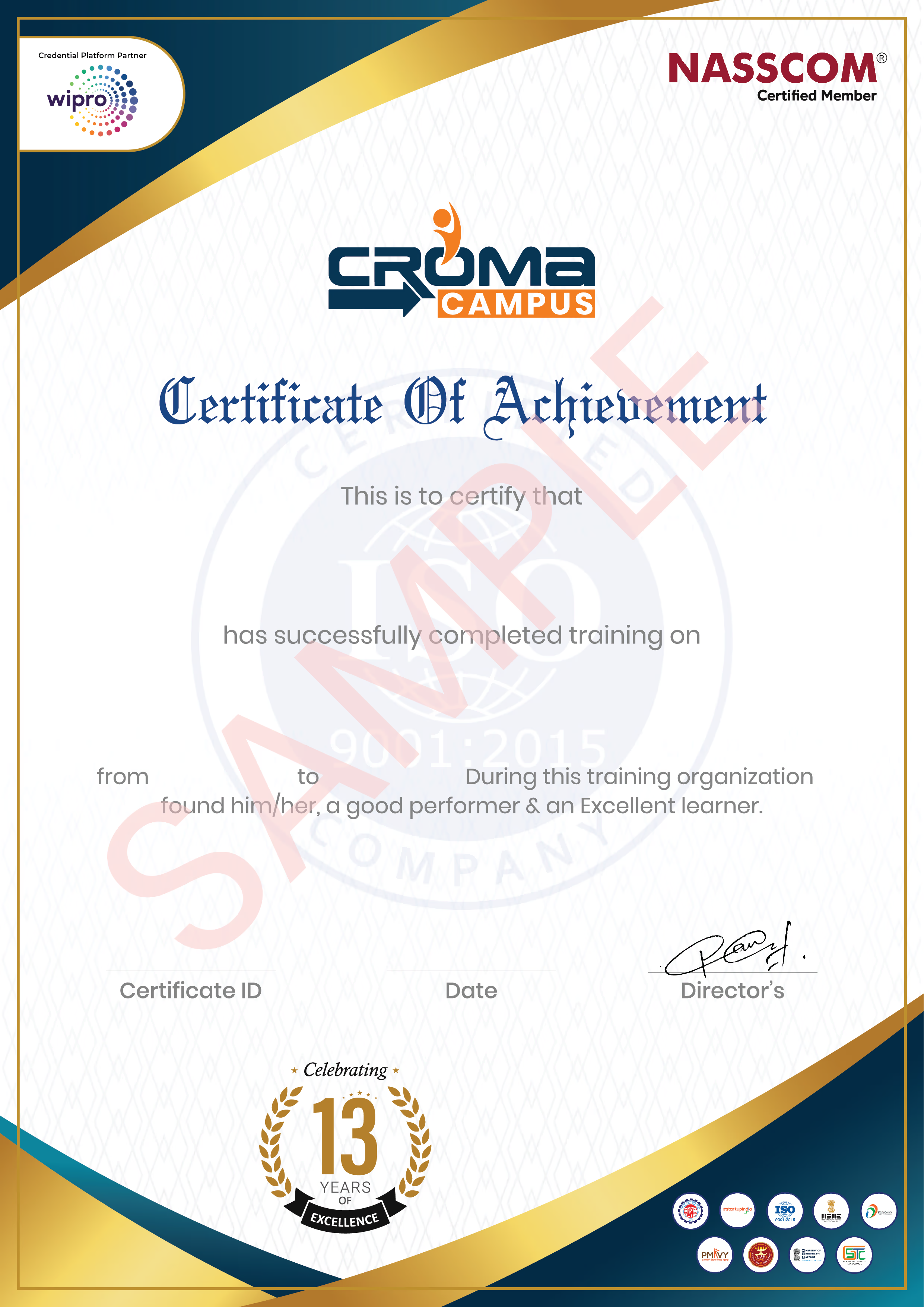
Certification
Each certification associated with the program is affiliated with the top universities providing edge to gain epitome in the course.
Showcase your Course Completion Certificate to Recruiters
-
 Training Certificate is Govern By 12 Global Associations.
-
Training Certificate is Powered by “Wipro DICE ID”
-
Training Certificate is Powered by "Verifiable Skill Credentials"

.webp)


Join us for a Free Demo
Share some of your details and we will be in touch with you for demo details, and know about Batches Available with us!


Get Latest Salary Trends

For Voice Call
+91-971 152 6942For Whatsapp Call & Chat
+91-9711526942
Ask For
DEMO


 Master in Cloud Computing Training